- 您现在的位置:买卖IC网 > Sheet目录1991 > CS5550-ISZR (Cirrus Logic Inc)IC ADC 2CH LOW-COST 24-SSOP
CS5550
DS630F1
5
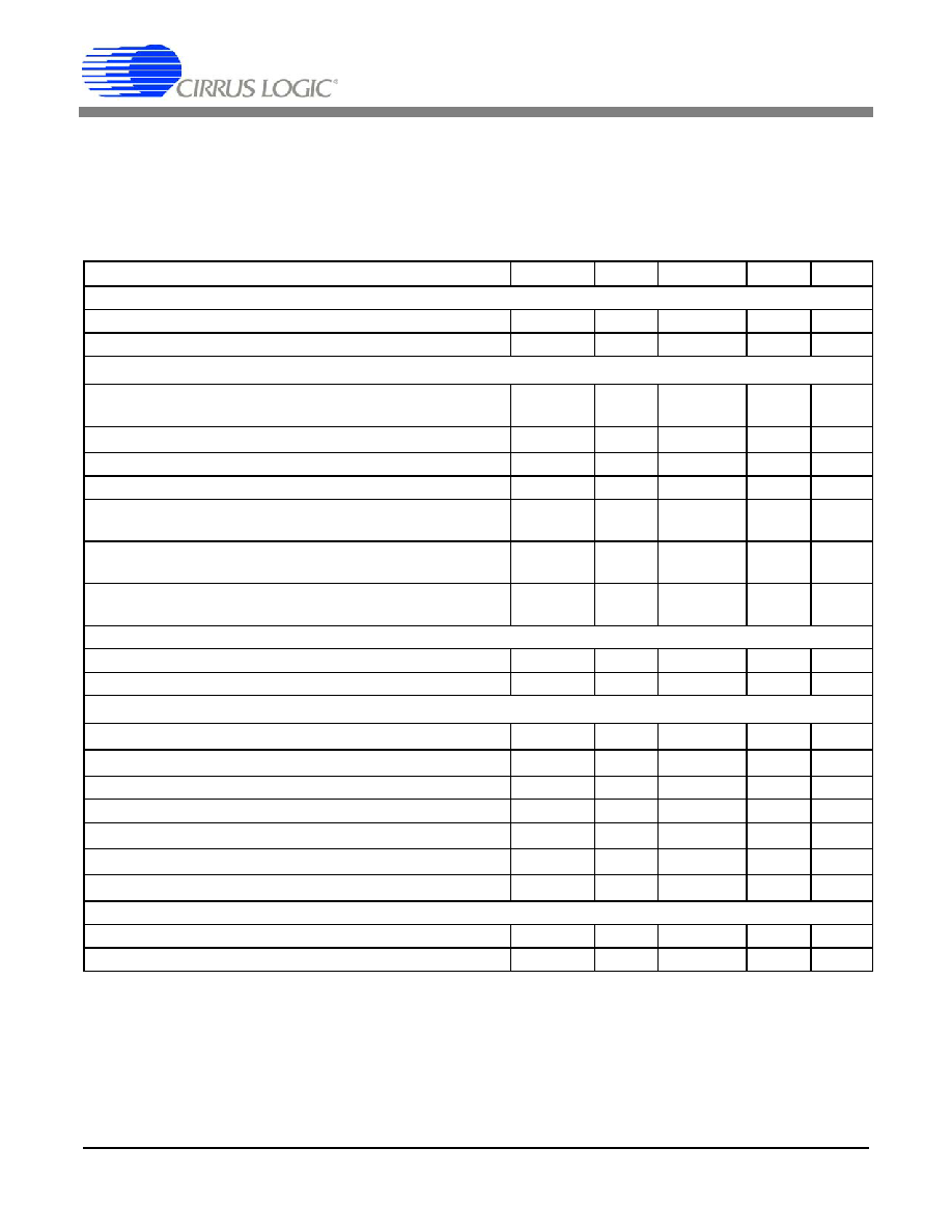
2. CHARACTERISTICS/SPECIFICATIONS
Min / Max characteristics and specifications are guaranteed over all Operating Conditions.
Typical characteristics and specifications are measured at nominal supply voltages and TA = 25°C.
DGND = 0 V. All voltages with respect to 0 V.
ANALOG CHARACTERISTICS
Notes: 1. Applies after system calibration
2. Effective Input Impedance (EII) is determined by clock frequency (DCLK) and Input Capacitance (IC).
EII = 1/(IC*DCLK/4). Note that DCLK = MCLK / K.
Parameter
Symbol
Min
Typ
Max
Unit
Accuracy (Both Channels)
Common Mode Rejection
(DC, 50, 60 Hz)
CMRR
80
-
dB
Offset Drift
-
5
-
nV/°C
Analog Inputs (AIN1
±)
Differential Input Voltage Range
(Gain = 10)
{(AIN1+) - (AIN1-)}
(Gain = 50)
AIN1
0
-
500
100
mVP-P
Total Harmonic Distortion
THD1
80
-
dB
Common Mode + Signal
Both Gain Ranges
-0.25
-
VA+
V
Crosstalk with AIN2± at Full Scale
(50, 60 Hz)
-
-115
dB
Input Capacitance
(Gain = 10)
(Gain = 50)
IC1
-
25
-
pF
Effective Input Impedance
(Gain = 10)
(Note 2)
(Gain = 50)
EII1
30
-
k
k
Noise (Referred to Input)
(Gain = 10)
(Gain = 50)
N1
-
22.5
4.5
Vrms
Accuracy
Bipolar Offset Error
(Note 1)
VOS
-
±0.001
%F.S.
Full-Scale Error
(Note 1)
FSE
-
±0.001
%F.S.
Analog Inputs (AIN2
±)
Differential Input Voltage Range
{(AIN2+) - (AIN2-)}
AIN2
0-
500
mVP-P
Total Harmonic Distortion
THD2
65
-
dB
Common Mode + Signal
-0.25
-
VA+
V
Crosstalk with AIN1± at Full Scale
(50, 60 Hz)
-
-70
dB
Input Capacitance
(Gain = 10)
IC2
-0.2
-
pF
Effective Input Impedance (Note 2)
(Gain = 10)
EII2
5-
-
M
Noise (Referred to Input)
(Gain = 10)
N2
--
150
Vrms
Accuracy
Bipolar Offset Error
(Note 1)
VOS
-
±0.01
%F.S.
Full-Scale Error
(Note 1)
FSE
-
±0.01
%F.S.
发布紧急采购,3分钟左右您将得到回复。
相关PDF资料
CS5565-ISZ
IC ADC DELTA-SIGMA 24BIT 24-SSOP
CY28317PVXC-2
IC CLK FTG VIA PL/E133T 48SSOP
CY28323OXC
IC CLOCK BROOKDALE GPENT4 48SSOP
CY28354OXC-400
IC BUFF 273MHZ 4DDR DIMM 48SSOP
CY28378OXC
IC CLOCK CK408/TITAN 845 48SSOP
CY284108ZXC
IC CLOCK SERV CK410B 56TSSOP
CY28410OXC-2
IC CLOCK CK410 GRANTSDALE 56SSOP
CY28410OXC
IC CLOCK CK410 GRANTSDALE 56SSOP
相关代理商/技术参数
CS5-56
制造商:SUPERWORLD 制造商全称:Superworld Electronics 功能描述:POWER TRANSFORMER
CS5560
制造商:CIRRUS 制造商全称:Cirrus Logic 功能描述:【2.5 V / 5 V, 50 kSps, 24-bit, High-throughput ツヒ ADC
CS5560_08
制造商:CIRRUS 制造商全称:Cirrus Logic 功能描述:±2.5 V / 5 V, 50 kSps, 24-bit, High-throughput ΔΣ ADC
CS5560_09
制造商:CIRRUS 制造商全称:Cirrus Logic 功能描述:±2.5 V / 5 V, 50 kSps, 24-bit, High-throughput ΔΣ ADC
CS5560-ISZ
功能描述:模数转换器 - ADC 24-Bit 50 kSps ADC RoHS:否 制造商:Texas Instruments 通道数量:2 结构:Sigma-Delta 转换速率:125 SPs to 8 KSPs 分辨率:24 bit 输入类型:Differential 信噪比:107 dB 接口类型:SPI 工作电源电压:1.7 V to 3.6 V, 2.7 V to 5.25 V 最大工作温度:+ 85 C 安装风格:SMD/SMT 封装 / 箱体:VQFN-32
CS5560-ISZR
功能描述:模数转换器 - ADC IC 50 DSDS 24-bit Mux DS ADC RoHS:否 制造商:Texas Instruments 通道数量:2 结构:Sigma-Delta 转换速率:125 SPs to 8 KSPs 分辨率:24 bit 输入类型:Differential 信噪比:107 dB 接口类型:SPI 工作电源电压:1.7 V to 3.6 V, 2.7 V to 5.25 V 最大工作温度:+ 85 C 安装风格:SMD/SMT 封装 / 箱体:VQFN-32
CS5561-ISZ
功能描述:IC ADC DELTA-SIGMA 24BIT 24-SSOP RoHS:是 类别:集成电路 (IC) >> 数据采集 - 模数转换器 系列:- 产品培训模块:Lead (SnPb) Finish for COTS
Obsolescence Mitigation Program 标准包装:2,500 系列:- 位数:12 采样率(每秒):3M 数据接口:- 转换器数目:- 功率耗散(最大):- 电压电源:- 工作温度:- 安装类型:表面贴装 封装/外壳:SOT-23-6 供应商设备封装:SOT-23-6 包装:带卷 (TR) 输入数目和类型:-
CS5561-ISZR
制造商:Cirrus Logic 功能描述: